Adding an S/PDIF output to your Super NES
Adding a digital audio out to the SNES isn't difficult. (Well, if you're not afraid of a soldering iron.) The DSP in the SNES outputs a raw 32kHz 16-bit stereo signal. In order to get this signal into a consumer digital receiver it needs to be reformatted to the S/PDIF standard.
To create an S/PDIF out I'm using a digital transmitter made by Cirrus Logic. In particular the CS8405A-CS (SOIC), which you can get for around 3 USD. The CS8405A will take a raw data stream and reformat it to the IEC60958 specification.
1. Determining your APU type
Before you go any further, you need to find out what kind of APU you have.
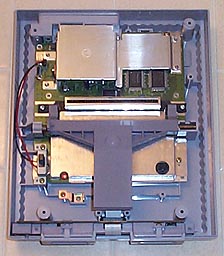
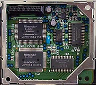
I'm assuming you already have a 4.5mm Nintendo screwdriver bit, otherwise you're going to have some difficulty getting into your SNES. Remove the six screws from the bottom, then take the top of the deck off. If you live in North America, you'll likely be presented with one of the two images:
Look in the upper right corner. If you see a silver box that reads SHVC-SOUND, then you have one of the first SNES decks.
If you see two chips under the heatsink, then you have a revised SNES.
If you see only one chip under the heatsink, then you have the last revision of the APU. These units are rarely found in North America, but seem to be popular in Europe.
2. Taking everything apart
2.1 Removing the APU module
If you have the old style SNES, you'll need to remove the APU module in order to get to the DSP. Do this by removing the two screws in the opposite corners of the module, then pulling the module straight up to disconnect it from the main board.
Next you'll need to take the lid off the underside of the module (the side with the 24-pin connector). Slide a small standard screwdriver under the lip on one of the sides. Carefully push the lip off the module. Do this on each side until the lid comes off.
2.2 Getting the heatsink off
If you have the newer style SNES, you're going to need to get the heatsink off in order to get to the DSP. If you have the older style with the APU module, removing the heatsink isn't necessary, but it could make adding the output connector easier.
The heatsink is held on by three or four screws on the underside of the mainboard. So to get it off you'll need to take everything out.
There are seven or nine screws holding the mainboard in place (four silver, three or five gold). You'll need to remove the power switch to get one of the gold screws out.
Before removing the mainboard from the SNES case, remove the screw holding the voltage regulator to the heatsink. Flip the board over and remove the screws holding the heatsink on.
2.3 Toss the RF module
When was the last time you used the RF adaptor? If your home theater system is sophisticated enough that you need an S/PDIF out, then you probably won't be using the RF adaptor with your TV. I mention this because the RF out is a good place to put your S/PDIF connector. This way you don't need to drill any new holes in your case.
The shielded RF box thingy is held on by three screws, one on the top and two on the bottom. Once you take the screws out you'll need to use a soldering iron to disconnect the four pins from the main board.
3. Wiring it up
3.1 Mating the two chips
Rather than draw up a schematic, I've made a table of the pins you need to connect. The S-DSP column contains the pins you need to connect to if you have a two chip APU, and the S-APU column contains the pins you need to connect to if you have a single chip APU.
S-DSP	S-APU	CS8405A 	Pin
33 	3 	+5VDC 		1    	COPY/C 	[CS bit 2] Copyright = 1 (allow copying)
				2 	VL2+
				3 	EMPH 	[CS bits 3-5] Emphasis = 0 (no emphasis)
				4 	SFMT0 	Data input is 16-bits right justified
				5 	SFMT1 	" "
				6 	VD+
				11 	TCBLD 	TCBL is output
				20 	VL3+
				23 	VL+
				24 	H/S 	Select hardware mode for controlling channel-status (CS) bit
				27 	VL4+

52 	95 	GND(1) 		7 	DGND4
				8 	DGND3
				10 	APMS 	Set data input to slave mode (input is controlled by ISCLK)
				16 	CEN 	Select hardware mode A for setting channel status
				17 	V 	[Validity bit] Sub-frame contains valid sample data
				18 	U 	[User bit] Always 0
				19 	AUDIO(2) 	[CS bit 1] Non-Audio = 0 (block contains audio data)
				22 	DGND
				28 	ORIG 	[CS bits 0 & 15] Pro = 0 (consumer format), L (Category Code MSB) = 0 (original recording)

47 	16 	RST 		9 	RST 	Reset
43 	94 	32kHz 		12 	ILRCK 	Left/Right sample clock
42 	92 	1.536MHz 	13 	ISCLK 	Sample bit clock
44 	93 	DATA 		14 	SDIN 	Sample data input
78 	52  	8.192MHz    	21 	OMCK 	Master clock

Not connected 			15 	TCBL
				25 	TXN

Output 				26 	TXP 	S/PDIF output
1 Instead of grounding to the DSP, I soldered pin 28 of the CS8405A to the mainboard and tied all grounds there. This doubled as a way to anchor the chip.
2 The documentation for the CS8405A would indicate that this pin needs to be set high, but this appears to be incorrect.
3.2 Half a bubble is close enough
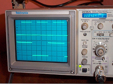
Using the clock signals from the DSP results in synchronous operation in the CS8405A, but the output from the DSP isn't exactly 32kHz.
As you can see here, my SNES is outputting samples at about 32040Hz. (Though you can't see the detail in this picture, the upper trace is of the 16-bit samples and the lower trace is the sample clock.) This shouldn't be a problem unless you're trying to sync S/PDIF devices or your input device insists on using its own clock.
The CS8405A allows for asynchronous operation. So, if necessary, you can supply your own master clock (OMCK) by using a more accurate crystal to ensure 32kHz output. However, doing so will result in samples being dropped or repeated.
3.3 Connecting the output
You can decide on the output connector you want to use. If you're going to use a Toslink (optical) connector, the TXP pin can be used to directly drive the output circuit.
If you want to use a coaxial (RCA) output, you'll need to throw in a couple of resistors to drop the voltage down to the consumer grade 0.5 volts.

4. Put it back together
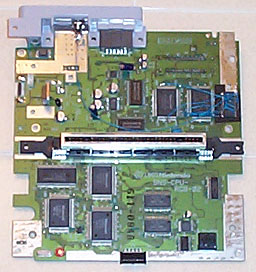
Here's the final product. I don't have a very good digital camera, or I'd have put up better pictures.
Hope you remember where all those screws went. :)
Copyright ©2003 Alpha-II Productions
Using a CS8406
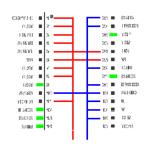
As the CS8405 is getting hard to get these days, here's a connection diagram for the CS8406.
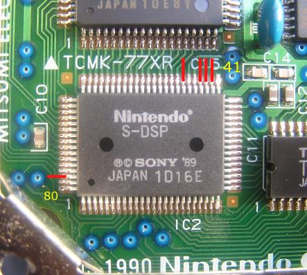
And I thought a pic of the pins on the DSP might be useful.
The clock, data, and reset pins are all in the same place. just a couple differences in what goes to ground / Vcc. In regards to the AUDIO pin note above, the CS8406 datasheet is corrected with the AUDIO line low for valid audio data.
I got so frustrated trying to solder wires to the DSP inside the APU can I ended up giving up on analog audio and lifting the pins. Don't do this! This will result in a nice black screen. It's all better now.


